- 您现在的位置:买卖IC网 > Sheet目录130 > DFLS1200-7 (Diodes Inc)DIODE SCHOTTKY 1A 200V PWRDI 123


DFLS1200
Document number: DS30628 Rev. 6 - 2
1 of 3
www.diodes.com
October 2008
? Diodes Incorporated
DFLS1200
PowerDI is a registered trademark of Diodes Incorporated.
1.0A HIGH VOLTAGE SCHOTTKY BARRIER RECTIFIER ?
123
PowerDI
Features
?
Guard Ring Die Constructi
on for Transient Protection
?
Low Power Loss, High Efficiency
?
Patented Interlocking Clip Design for High Surge Current
Capacity
?
Lead Free Finish, RoHS Compliant (Note 4)
?
"Green" Molding Compound (No Br, Sb)
?
Qualified to AEC-Q101 Standards for High Reliability
Mechanical Data
?
Case: PowerDI
?123
?
Case Material: Molded Plastic,
"Green" Molding Compound.
UL Flammability Classification Rating 94V-0
?
Moisture Sensitivity: Level 1 per J-STD-020D
?
Terminal Connections: Cathode Band
?
Terminals: Finish – Matte Ti
n annealed over Copper Leadframe.
Solderable per MIL-STD-202, Method 208
?
Marking Information: See Page 2
?
Ordering Information: See Page 2
?
Weight: 0.01 grams (approximate)
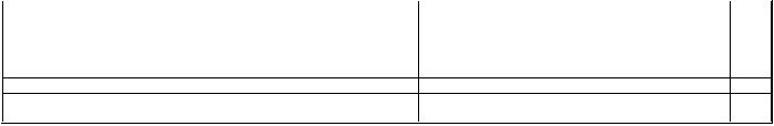
Maximum Ratings
@TA
= 25°C unless otherwise specified
Single phase, half wave, 60Hz, resistive or inductive load.
For capacitance load, derate current by 20%.
Characteristic
Symbol
Value
Unit
Peak Repetitive Reverse Voltage
Working Peak Reverse Voltage
DC Blocking Voltage
VRRM
VRWM
VR
200
V
RMS Reverse Voltage
VR(RMS)
141
V
Average Forward Current
IF(AV)
1.0
A
Non-Repetitive Peak Forward Surge Current 8.3ms
Single Half Sine-Wave Superimposed on Rated Load
IFSM
40
A
Thermal Characteristics
Characteristic
Symbol Typ
Max
Unit
Thermal Resistance Junction to Ambient (Note 1)
RθJA
132
?
°C/W
Thermal Resistance Junction to Soldering Point (Note 2)
RθJS
?
7
°C/W
Operating and Storage Temperature Range
TJ, TSTG
-65 to +175
°C
Electrical Characteristics
@TA
= 25°C unless otherwise specified
Characteristic
Symbol
Min
Typ
Max
Unit
Test Condition
Reverse Breakdown Voltage (Note 3)
V(BR)R
200
?
?
V
IR
= 8
μA
Forward Voltage
VF
?
?
0.85
V
IF
= 1.0A
Leakage Current (Note 3)
IR
?
?
2
μA
VR
= 200V, T
A
= 25
°C
Total Capacitance
CT
?
23
?
pF
VR
= 5VDC, f = 1MHz
Notes: 1. Part mounted on FR-4 board with 2 oz., minimum recommended copper pad layout, which can be found on our website at
http://www.diode
s.com/datasheets/ap02001.pdf. TA
= 25°C
2. Theoretical RθJS
calculated from the top center of the die straig
ht down to the PCB/cathode tab solder junction.
3. Short duration pulse test used to minimize self-heating effect.
4. EU Directive 2002/95/EC (RoHS). All applicable RoHS exemptions applied, see EU Directive 2002/95/EC Annex Notes.
Top View
发布紧急采购,3分钟左右您将得到回复。
相关PDF资料
DFLS120L-7
DIODE SCHOTTKY 20V 1A POWERDI123
DFLS130-7
DIODE SCHOTTKY 30V 1A POWERDI123
DFLS130L-7
DIODE SCHOTTKY 30V 1A POWERDI123
DFLS140-7
DIODE SCHOTTKY 40V 1.1A PWRDI123
DFLS140L-7
DIODE SCHOTTKY 40V 1A POWERDI123
DFLS160-7
DIODE SCHOTTKY 1A 60V POWERDI123
DFLS2100-7
DIODE SCHOTKY 100V 2A POWERDI123
DFLS220L-7
DIODE SCHOTTKY 2A 20V PWRDI 123
相关代理商/技术参数
DFLS1200-7-CUT TAPE
制造商:DIODES 功能描述:DFLS1200 Series 200 V 1 A Schottky Barrier Rectifier Surface Mount - POWERDI-123
DFLS120L
制造商:未知厂家 制造商全称:未知厂家 功能描述:1.0A SURFACE MOUNT SCHOTTKY BARRIER RECTIFIER
DFLS120L_08
制造商:DIODES 制造商全称:Diodes Incorporated 功能描述:1.0A SURFACE MOUNT SCHOTTKY BARRIER RECTIFIER
DFLS120L_1
制造商:未知厂家 制造商全称:未知厂家 功能描述:1.0A SURFACE MOUNT SCHOTTKY BARRIER RECTIFIER
DFLS120L7
制造商:Diodes Incorporated 功能描述:
DFLS120L-7
功能描述:肖特基二极管与整流器 1A 20V RoHS:否 制造商:Skyworks Solutions, Inc. 产品:Schottky Diodes 峰值反向电压:2 V 正向连续电流:50 mA 最大浪涌电流: 配置:Crossover Quad 恢复时间: 正向电压下降:370 mV 最大反向漏泄电流: 最大功率耗散:75 mW 工作温度范围:- 65 C to + 150 C 安装风格:SMD/SMT 封装 / 箱体:SOT-143 封装:Reel
DFLS120L-7-CUT TAPE
制造商:DIODES 功能描述:DFLS120L Series 20 V 1 A Surface Mount Schottky Barrier Rectifier-PowerDI-123
DFLS130
制造商:DIODES 功能描述:1.0A SCOTTKY RECTIFIER POWER TM 123
